From PCB to Flyback Power Supply, Switching Power Supply Design
2022-02-12 09:57:10
Talk about years of experience in the design of switching power supply, from the design of switching power supply printed circuit board, printed circuit board wiring, printed circuit board copper skin alignment, the application of aluminum substrate and multilayer printed circuit board in switching power supply, to the duty cycle of flyback power supply.
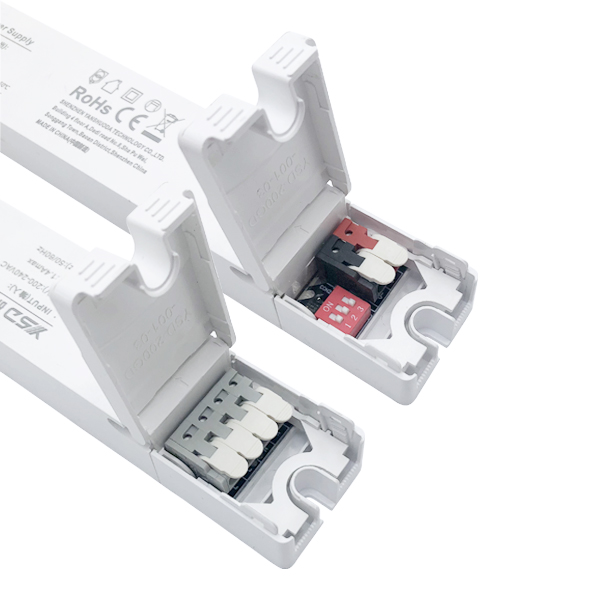
1.Design of LED power supply printed board
Let's start with a description of the design and production process of
LED switching power supply, starting with the design of the printed circuit board. Switching power supply works in high frequency, high pulse state, belongs to a relatively special type of analog circuit. Board layout must follow the principles of high-frequency circuit wiring.
The pulse voltage lines are as short as possible, from the input switching tube to the transformer and from the output transformer to the rectifier. Pulse current loop as small as possible, such as the input filter capacitor positive to the transformer to the switch tube return capacitor negative. From the output of the transformer to the rectifier to the output capacitor to the output capacitor and then return to the transformer circuit X capacitor should be as close as possible to the input of the switching power supply, the input line should avoid parallel to other circuits, should be avoided. y capacitor should be placed in the chassis ground terminal or FG connection. The common touch inductor should be kept at a certain distance from the transformer to avoid magnetic coupling. If it is not good to handle, a shield can be added between the common touch inductor and the transformer. The above items have a greater impact on the EMC performance of the switching power supply.
Output capacitors can generally be used two, one near the rectifier, the other should be close to the output terminals, can affect the power supply output ripple indicators, two small-capacity capacitors in parallel should be better than a large-capacity capacitors. Heat generating devices and electrolytic capacitors to maintain a certain distance to prolong the life of the machine, electrolytic capacitors are the bottleneck of the life of the switching power supply, such as transformers, power tubes, high-power resistors and electrolytic distance to maintain the electrolytic, electrolytic space must be left between the heat dissipation, conditions allow it to be placed in the air inlet.
To pay attention to the control section: high impedance weak signal circuit connections should be as short as possible such as sampling feedback loop, in processing to try to avoid its interference, current sampling signal circuit, especially the current control type circuit, otherwise there will be some unexpected accidents.
2.Principles of printed board wiring
Line spacing: With the continuous improvement of the printed circuit board manufacturing process, the general processing factory manufacturing line spacing equal to or even less than 0.1mm has been no problem, fully able to meet most applications.Considering the components and production process used in switching power supply, double-sided minimum line spacing set to 0.3mm, single-sided minimum line spacing set to 0.5mm, pads and pads, pads and holes or holes and holes, the minimum spacing set to 0.5mm, can avoid the "bridging" phenomenon during the welding operation.Therefore, most board factories can easily meet the production requirements and achieve a reasonable wiring density and a more economical cost.
The minimum line spacing is only suitable for signal control circuits and low-voltage circuits with voltages lower than 63V. When the voltage between lines is greater than this value, the line spacing can generally be taken in accordance with the 500V/1mm empirical value.
In view of the fact that there are some relevant standards have clearer regulations on the line spacing, it is necessary to strictly follow the standards, such as the AC input connected to the fuse ports. Some LED power supplies have high volume requirements, such as modular power supply. General transformer input side line spacing of 1mm practice has proved to be feasible. For AC input, (isolated) DC output power products, more stringent regulations for the safety spacing to be greater than or equal to 6mm. Of course, this is determined by the relevant standards and implementation methods. General safety spacing can be used as a reference by the distance between the two sides of the feedback optocoupler, the principle is greater than or equal to this distance. Can also be slotted on the printed board below the optocoupler, so that the creepage distance is increased to meet the insulation requirements. General switching power supply AC input side alignment or board components from the non-insulated shell, heat sink spacing should be greater than 5mm, the output side alignment or device from the shell or heat sink spacing should be greater than 2mm, or in strict accordance with safety standards.
Commonly used methods: The above-mentioned method of slotting the circuit board is suitable for some occasions where the spacing is not enough. Incidentally, the method is also commonly used as a protective discharge gap, commonly found at the tail board of TV picture tube and power supply AC input. The method is widely used in the modular power supply, and good results can be obtained under the conditions of potting.
Method 2: pad insulation paper, can be used green shell paper, mylar film, polytetrafluoroethylene orientation film and other insulating materials. General power supply with green shell paper or polyester film pad in the circuit board between the metal chassis, this material has a high mechanical strength, a certain resistance to moisture. Teflon oriented film is widely used in modular power supply because of its high temperature resistance. Insulation film can also be padded between components and surrounding conductors to improve the insulation resistance.
Note: Some device insulation covers cannot be used as insulation media to reduce the safety spacing, such as the outer skin of electrolytic capacitors, which may be subject to thermal contraction under high temperature conditions. Space should be left at the front of the large electrolytic explosion-proof tank to ensure unobstructed voltage relief for electrolytic capacitors in extraordinary conditions.
3.Notes on copper skin alignment of printed circuit boards
Alignment current density: most electronic circuits now use insulated board bound copper composition. Commonly used circuit board copper skin thickness of 35μm, the alignment can be taken in accordance with 1A/mm empirical value of current density value. To ensure the mechanical strength of the alignment principle line width should be greater than or equal to 0.3mm (other non-power circuit board may be a minimum line width will be small). Some). Copper thickness of 70μm circuit board is also common in the switching power supply, then the current density can be higher.
Now commonly used circuit board design tools software generally have a design specification items, such as line width, line spacing, pad over hole size and other parameters can be set. In the design of the circuit board, the design software can be automatically implemented in accordance with the specifications, which can save a lot of time, reduce part of the workload and reduce the error rate.
General requirements for the reliability of the higher line or wiring line density can be used double-sided. It is characterized by moderate cost, high reliability, and can be used in most applications.
Module power supply ranks also have some products using multilayer board, mainly to facilitate the integration of transformers inductors and other power devices, optimize wiring, power tube heat dissipation, etc.. With the advantages of beautiful process consistency, transformer heat dissipation is good, but its disadvantage is the higher cost, less flexible, only suitable for industrial production.
The market circulation of general-purpose switching power supply almost all use a single-sided circuit board, which has the advantage of low cost, in the design and production process to take some measures to ensure its performance.
4.Design of single-sided printed boards
Because of its low cost and easy manufacturing characteristics, the single panel is widely used in the switching power supply circuit, because it has only one side bound copper, the electrical connection of the device, mechanical fixing are dependent on that layer of copper skin, must be handled with care.
To ensure good performance of the mechanical structure of the welding, single panel pad should be slightly larger to ensure that the copper skin and the substrate of good binding force, and not to be subject to vibration when the copper skin stripped, broken off. The general width of the solder ring should be greater than 0.3mm. pad hole diameter should be slightly larger than the device pin diameter, but should not be too large to ensure that the distance between the pins and pads by the solder connection is the shortest, the size of the disk hole to not hinder the normal check for the degree, the pad hole diameter is generally larger than the pin diameter 0.1-0.2mm. multi-pin devices to ensure smooth checking, can also be larger.
Single panel components should be close to the circuit board.Need to overhead heat dissipation components, to add sleeves on the pins between the device and the circuit board, which can play a dual role of supporting the device and increasing insulation. To minimize or avoid the impact of external forces on the connection between the solder plate and the pin, to enhance the solidity of the welding. Line board weight components can be increased to support the connection point, can strengthen the strength of the connection between the board and the line, such as transformers, power devices heat sink.
Double-sided pads due to holes have been metalized for higher strength, solder ring can be smaller than a single panel, pad hole aperture can be slightly larger than the diameter of the pin, because in the welding process is conducive to solder solution through the solder hole penetration to the top pad, to increase the reliability of welding. But there is a disadvantage, if the hole is too large, wave welding in the jet tin impact part of the device may float up, producing some defects.
The processing of high-current alignment, line width can be handled in accordance with the former post, such as width is not enough, generally can be used in the alignment of tin plating to increase the thickness of the solution, there are several methods.
1, the alignment will be set to pad properties, so that the alignment will not be covered by solder resist when the circuit board manufacturing, hot air leveling will be tinned.
2、Place pads at the wiring, the pad will be set to the shape of the need for the alignment, the pad hole should be set to zero.
3, In the solder resist layer to place the line, this method is the most flexible, but not all circuit board manufacturers will understand your intention, need to use text to explain. In the solder resist layer to place the part of the line will not be coated with solder resist.
Several methods of line tinning as above, it should be noted that if a very wide alignment all tinned, after welding, will bond a lot of solder, and the distribution is very uneven, affecting the aesthetics. Generally can use a long thin strip of tinning width in 1 ~ 1.5mm, the length can be determined according to the line, tinning part of the interval 0.5 ~ 1mm double-sided circuit board provides a great deal of selectivity for the layout and alignment , can make the wiring more reasonable. On grounding, power ground and signal ground must be separated, two ground can be converged at the filter capacitor to avoid large pulse current through the signal ground connection and lead to unstable accidental factors, signal control circuit try to use a little grounding method, there is a trick, try to place non-grounded alignment in the same wiring layer, and finally in the other layer to lay the ground. The output line generally passes through the filter capacitor first, and then to the load, the input line must also pass through the capacitor first, and then to the transformer, the theoretical basis is to let the ripple current are through the brigade filter capacitor.
Alignment from a wiring layer to another wiring layer is generally connected by a hole, should not be realized through the device pin pads, because in the insertion of devices may destroy this connection, there is a current through each 1A, there should be at least 2 holes, the principle of aperture to be greater than 0.5mm when over the hole, generally 0.8mm to ensure processing reliability.
Device heat dissipation, in some low-power power supply, the circuit board alignment can also be a heat dissipation function, which is characterized by the alignment as wide as possible to increase the heat dissipation area, and not coated with solder resist, the conditions can be uniformly placed over the hole, to enhance thermal conductivity.
5.Application of aluminum substrate and multilayer printed circuit board in the switching power supply
Aluminum substrate by its own construction, has the following characteristics: thermal conductivity is very good, single-sided bonded copper, devices can only be placed in the bonded copper surface, can not open the electrical connection hole so can not be placed in accordance with the single panel jumper.
Aluminum substrate are generally placed on the SMD devices, switching tubes, output rectifier tube through the substrate to conduct heat out, thermal resistance is very low, can achieve higher reliability. Transformer using flat SMD structure, can also be heat dissipation through the substrate. The same specification transformer using aluminum substrate structure can get a larger output power. Aluminum substrate jumper can be used to bridge the way to deal with. Aluminum substrate power supply is generally composed of two printed boards, another board to place the control circuit, the two boards are physically connected to form one.
Due to the excellent thermal conductivity of aluminum substrate, in a small amount of manual welding is more difficult, the solder cooling too fast, there is a simple and practical way to solve the problems which are easy to appear, using an iron (preferably with temperature adjustment function), turn over, ironing face up and fixed, the temperature is adjusted to about 150 ℃, the aluminum substrate on top of the iron, heating for a period of time, and then according to the conventional method will be attached to the components and welding, the temperature of the iron to the device is easy to weld appropriate, too high may be when the device damage, and even aluminum substrate copper peel, the temperature is too low welding effect is not good, to be flexible.
Switching power supplies are divided into two forms: isolated and non-isolated. Isolated power supplies can be divided into two main categories according to the form of structure: forward-excited power supply and flyback power supply. Flyback power supply refers to the primary side of the transformer conduction when the secondary side is cut off, the transformer energy storage. When the primary side cutoff, the secondary side conduction, energy release to the load working state, the general conventional flyback power supply single tube more, double tube is not common. Forward-excited refers to the primary side of the transformer conduction at the same time the secondary side of the induction of the corresponding voltage output to the load, the energy is directly transferred through the transformer. According to the specifications can be divided into conventional flyback, including single-tube flyback, double-tube flyback. Half-bridge and bridge circuits are all forward-excited circuits.
Forward circuits and flyback circuits have their own characteristics and can be used flexibly in the process of circuit design to achieve optimal cost performance. Generally, flyback can be used in low-power applications. Slightly high-power can be used single-tube forward circuit, medium power can be used double-tube forward circuit or half-bridge circuit. At low voltage, a push-pull circuit is used, which is the same as the half-bridge operating state. High power output, the general use of bridge circuit, low-voltage can also be used push-pull circuit. Flyback power supply are widely used in small and medium power supplies because of their simple structure, eliminating an inductor of about the same size as a transformer.
Transformer leakage inductance flyback power supply is a very critical parameter, because the flyback power supply requires the transformer to store energy, to make full use of the transformer core, generally have to open the air gap in the magnetic circuit, the purpose is to change the slope of the core hysteresis line, so that the transformer can withstand large pulse current shock, without the core into a saturated non-linear state, the air gap in the magnetic circuit in a high reluctance state, in the magnetic circuit to produce leakage is much larger than a completely closed magnetic circuit.
The coupling between the initial pole of the transformer is also a key factor in determining the leakage inductance, to make the initial pole coil as close as possible, sandwich winding method can be used, but this will make the transformer distribution of capacitance increases. Selection of cores try to use a relatively long window core, can reduce leakage inductance, such as the use of EE, EF, EER, PQ type core effect is better than EI type.
Regarding the duty cycle of flyback power supply,the maximum duty cycle of flyback power supply should be less than 0.5, otherwise the loop is not easy to compensate. Duty cycle is determined by the ratio of primary and secondary turns of the transformer. First determine the reflection voltage (output voltage through the transformer coupling reflected to the original side of the voltage value), in a certain voltage range, the reflection voltage increases the operating duty cycle increases, the switching tube loss is reduced. Reflected voltage decreases, the duty cycle decreases and the switching tube loss increases. Of course, this is also a prerequisite, when the duty cycle increases, it means that the output diode conduction time is shortened, in order to maintain output stability, more often than not will be guaranteed by the output capacitor discharge current, the output capacitor will be subject to greater high-frequency ripple current flushing, and make it heat up, which is not allowed under many conditions. Duty cycle increase, change the transformer turns ratio, will make the transformer leakage inductance increase, so that its overall performance, when the leakage inductance energy is large to a certain extent, can fully offset the low loss brought about by the large duty cycle of the switching tube, when there is no longer the significance of increasing the duty cycle, and may even be too high because of leakage inductance anti-peak voltage and breakdown of the switching tube. Due to the large leakage inductance, may make the output ripple, and some other electromagnetic indicators become worse. When the duty cycle is small, the switching tube through the current RMS value is high, the transformer primary current RMS value is large, reducing the efficiency of the converter, but can improve the working conditions of the output capacitor, reduce heat. How to determine the transformer reflection voltage (duty cycle).
6.Duty cycle of flyback power supply
Finally, talk about the duty cycle of the flyback power supply, duty cycle is also related to the selection of the switching tube voltage, there are some early flyback power supply using relatively low voltage switch tubes, such as 600V or 650V as the AC 220V input power switch, perhaps related to the production process at the time, high voltage tube, not easy to manufacture, or low voltage tube has a more reasonable conduction loss and switching characteristics, such as this line Reflected voltage can not be too high, otherwise, in order to make the switching tube work in the safe range, the power loss of the absorption circuit is also considerable. Practice has proved that the 600V tube reflection voltage should not be greater than 100V, 650V tube reflection voltage should not be greater than 120V, the leakage spike voltage value clamped at 50V when the tube has a 50V working margin. Now due to the improvement of the MOS tube manufacturing process, the general flyback power supply are used 700V or 750V or even 800-900V switching tube. Like this circuit, the ability to resist overvoltage some switching transformer reflection voltage can also be made higher, the maximum reflection voltage of 150V is more appropriate to obtain a better overall performance. 135V is recommended for PI's TOP chip using transient voltage suppression diode clamp. But his evaluation board is generally lower than this value of the reflection voltage in about 110V. These two types have advantages and disadvantages.
The first category: the disadvantage are weak resistance to overvoltage, duty cycle is small, transformer primary pulse current is large. The advantages are transformer leakage inductance is small, low electromagnetic radiation, high ripple index, small switching tube loss, conversion efficiency is not necessarily lower than the second category.
The second category: the disadvantages are switching tube loss is larger, transformer leakage inductance is larger, ripple is worse. The advantages are strong resistance to overvoltage, duty cycle is large, transformer losses are low, high efficiency.
There is another determining factor about reflected voltage of flyback power supply.The reflected voltage of the flyback power supply is also related to a parameter, that is the output voltage. The lower the output voltage the greater the transformer turns ratio, the greater the transformer leakage inductance, the higher the switching tube withstand voltage, the higher the risk of breakdown of the switching tube, the greater the power consumption of the absorption circuit, the risk of permanent failure of the absorption circuit power devices (especially the circuit using transient voltage suppression diodes). In the design of low-voltage output low-power flyback power supply optimization process must be handled carefully, there are several ways to deal with.
1.Using a large power level core to reduce leakage inductance, which can improve the conversion efficiency of low-voltage flyback power supply, reduce losses and output ripple, improve the crossover adjustment rate of multiple output power supplies, generally common in home appliances with switching power supplies, such as optical disc players, DVB set-top boxes, etc.
2.if the conditions do not allow to increase the core, can only reduce the reflection voltage, reduce the duty cycle. Reduce the reflection voltage can reduce leakage inductance but may make the power conversion efficiency is reduced, the two is a contradiction, there must be an alternative process to find a suitable point. In the process of transformer substitution experiment, you can detect the reflective voltage of the original side of the transformer, try to reduce the width of the reflective voltage pulse, and amplitude, can increase the safety margin of the converter work. Generally, the reflection voltage is more suitable at 110V.
3.In order to enhance coupling and reduce losses, new technologies and winding processes are used. Transformer to meet the safety specifications will take insulation measures between the primary and secondary sides, such as pad insulation tape, add insulation end air tape. These will affect the transformer leakage inductance performance, the reality of production can be used in the primary winding wrapped around the secondary winding method. Or secondary with triple insulated wire winding, the elimination of the initial level between the insulator can enhance coupling, or even a wide copper winding.
The core of the transformer of flyback power supply operates in a unidirectional magnetization state, so the magnetic circuit requires an open air gap, similar to a pulsating DC inductor. A part of the magnetic circuit through the air gap coupling. Why the principle of open air gap? As the power ferrite also has a nearly rectangular working characteristic curve (hysteresis), in the working characteristic curve Y axis indicates the magnetic induction strength (B), now the production process generally saturation point is more than 400mT , generally this value in the design of the value should be in 200-300mT , X axis indicates the magnetic field strength (H), this value is proportional to the magnetization current strength. Magnetic circuit open air gap is equivalent to the magnet hysteresis line to the X-axis tilt, in the same magnetic induction strength, it can withstand greater magnetization current, which is equivalent to the core to store more energy, this energy in the switching tube cut-off through the transformer secondary cascade to the load circuit, flyback power supply core open air gap has two roles. One is to transfer more energy, and the other is to prevent the core from entering saturation.
The transformer of flyback power supply works in a one-way magnetization state, not only to transfer energy through magnetic coupling, but also to assume the multiple roles of voltage conversion input and output isolation. So the air gap needs to be handled very carefully, the air gap is too large can make the leakage inductance becomes large, hysteresis loss increases, iron loss, copper loss increases, affecting the overall performance of the power supply. Air gap is too small may make the transformer core saturation, resulting in power damage.
The continuous and intermittent modes of flyback power supplies refer to the operating state of the transformer. At full load the transformer works in a mode of operation where energy is fully transferred, or not fully transferred. Generally to be designed according to the operating environment, the conventional flyback power supply should work in continuous mode, so that the loss of switching tubes and lines are small, and can reduce the operating stress of the input and output capacitors, but there are some exceptions to this.
Due to the characteristics of flyback power supply is also more suitable for design into high-voltage power supply, and high-voltage power transformers generally work in intermittent mode. Due to the manufacturing process characteristics, high reverse voltage diode, reverse recovery time is long and low speed, so in the current continuous state, the diode is recovered when there is forward bias, reverse recovery energy loss is very large, is not conducive to the improvement of converter performance, will reduce the conversion efficiency, rectifier tube serious heating, and even burn the rectifier tube. Because in intermittent mode, the diode is reverse biased under zero bias, the loss can be reduced to a relatively low level. Therefore, the high-voltage power supply works in intermittent mode, and the operating frequency cannot be too high.
The transformer of the flyback switching power supply should operate in continuous mode, which requires a relatively large winding inductance. Of course, there is a certain degree of continuity, and it is unrealistic to pursue absolute continuity too much, which may require a very large core and a very large number of turns, accompanied by large leakage inductance and distributed capacitance, which may not be worth the loss. So how to determine this parameter? Through repeated practice, it is concluded that at the nominal voltage input, the output should reach 50% to 60% transformer from intermittent, transition to continuous state is more appropriate. Or at the highest input voltage state, the transformer can transition to a continuous state when the output is fully loaded