How to Develop Switching Power Supply
2022-02-23 09:26:35
Switch power supply is difficult to be learned, and there are many things to consider. Generally speaking, some design cycles of the power supply are lagging behind the development of other module circuits. Because the switch power supply is the power supply system, we have to wait for other circuits to determine the supply voltage before we can design. The design cycle of power supply circuit is short and difficult, it is a challenge for power supply development engineers.
How to learn switch power supply?
Before learning switching power supply you need to know the basic circuit knowledge, such as analog circuits, electromagnetic fields, transformers, inductors, capacitors, etc. After these basics are understood, you can choose the right books about switching power supply knowledge to see. The first step is to understand the three basic topology circuits (BUCK/BOOST/BUCK-BOOST) and the principle of forward and flyback circuits. Then learn more about other parts of the circuit of the switching power supply, at least see a switching power supply diagram to know the role of each circuit. Finally you should know how to draw PCB, power supply board are generally used single panel, learning to use Altium Designer is enough, it is best to learn to use power simulation software which is saber simulation.
How to develop switching power supply?
The best way to learn to design switching power supply better and faster is to practice. It is best to enter a company that specializes in developing power supplies, not only to participate in projects, but also to be taught by professionals.
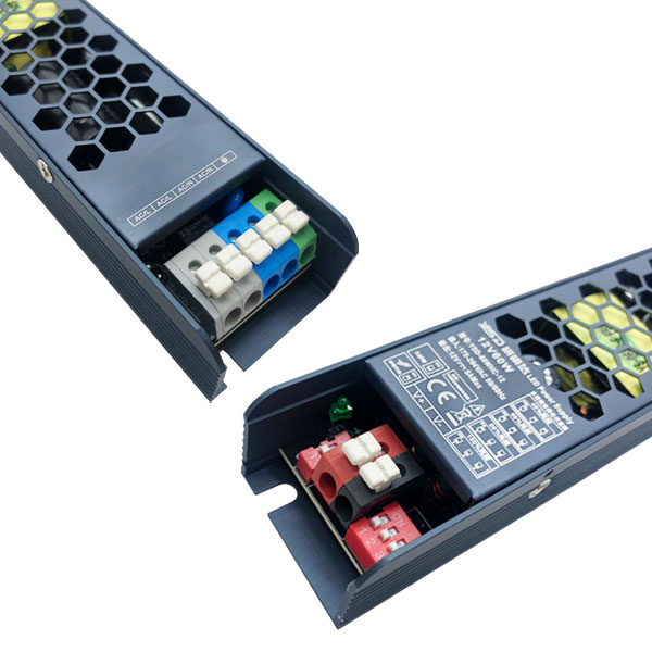
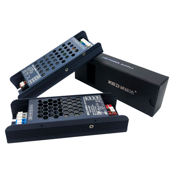
The following is a brief explanation of the components of a switching circuit.
Switching power supply probably has the following components.
①RCD buffer circuit: used to clamp the transformer leakage caused by the power switching tube Drain level voltage is too high;
② Output rectifier filter circuit: rectify AC=>DC output;
③Optical coupling feedback circuit: Optical coupling can achieve high voltage electromagnetic isolation;
④TL431 current feedback circuit: The part of the output voltage regulation feedback circuit;
⑤PWM chopper circuit: to adjust the output voltage by adjusting the duty cycle;
⑥ Input rectifier module: 220AC=>310DC;
⑦Input protection / EMC protection circuit: to prevent damage to the circuit when the circuit is abnormal, EMC considerations in harsh environments;
⑧Transformer: voltage conversion, energy conversion.
Next, talking about the design steps of SMPS of FLYBACK type.
1.Technical specifications: the designer is required to achieve the electrical performance, such as size, price and EMC operating conditions
2.Black box calculation: according to the use of mode to calculate the peak current, power and other elements of power supply work
3.Transformer design: according to the power and IC operating frequency to design the transformer primary winding, according to the output voltage and the number of output groups to design the secondary winding, and according to the actual elements to measure the wire gauge; (design focus: transformer coil leakage inductance to determine the quality of power)
4.Output rectifier filter: according to the selection of TOPO and output voltage, choose the most economical circuit rectifier filter. Filter capacitors to select a small ESR, or multiple capacitors in parallel to reduce ESR, reduce the output ripple;
5.IC: According to the output power selection IC, working at 67KHz, 30W-100W output is generally selected STA series
6.Controller / driver circuit: IC integrated control / drive system, so there is no need for separate design
7.Output feedback: When the output stability needs to consider the frequency response, the use of TL431 to establish a current feedback double loop than the use of three-type feedback loop design is simpler, easier to establish; (design difficulties: the feedback loop to determine the stability of the power supply)
8.Start circuit: IC VCC circuit and circuit design on each system module
9.Protection circuit: design over-current and over-voltage protection according to the peak current of the system
10.Thermal analysis and design: according to TOPO estimated efficiency of heat dissipation, to estimate the working temperature of key components, to determine whether the need to install a heatsink and the size of the heatsink; (heatsink size is related to the cost and PCB size, such as the case of oversized heatsink, you need to return to the previous stage to redesign)
11.PCB layout: pay attention to the circuit layout; (design difficulties: PCB layout determines the EMI system and the life of component)
①SMPS layout is generally divided into four major modes, input, power switch, output rectifier, output, the four should be separated from each other.
②Power and output should be separated.
12.Test:Test all performance indicators and improve them, and seek CI
13.EMI/RFI testing: EMI/RFI must meet the requirements of the exporting country.