Capacitive applications in power supply design
2020-01-03 16:44:07
Reference voltage source circuit
There are many ways to design a reference voltage source IC, each with specific advantages and disadvantages.
Reference voltage source based on zener diode
Deep buried zener reference voltage source is a relatively simple design. Zener (or avalanche) diodes have predictable reverse voltages that have excellent temperature stability and excellent time stability. These diodes usually have very low noise and very good time stability when kept in a small temperature range, so they are suitable for applications where the reference voltage changes are small.
Compared to other types of reference voltage source circuits, this stability can be attributed to a small number of components and a small chip area, and the construction of zener components is very delicate. However, it is common to see relatively large variations in the initial voltage and temperature drift. Circuits can be added to compensate for these defects, or a series of output voltages can be provided. Both shunt and series reference voltage sources use zener diodes.
Bandgap reference voltage source
Zener diodes can be used to produce high performance reference voltage sources but lack flexibility. Specifically, it requires a supply voltage of more than 7V and provides relatively little output voltage. In contrast, bandgap reference voltage sources can produce a wide variety of output voltages with a very small power margin (usually less than 100mV). Bandgap reference voltage sources can be designed to provide very accurate initial output voltages and very low temperature drift without the need for time-consuming in-service calibration.
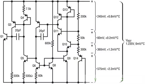
Bandgap operations are based on the basic characteristics of bipolar junction transistors. Figure 1 shows a basic bandgap reference voltage source. It can be seen that the VBE of a pair of mismatched bipolar junction transistors has a difference proportional to temperature. This difference can be used to produce a current that rises linearly with temperature. When this current is driven through a resistor and a transistor, the temperature variation of the transistor's base-emitter voltage with temperature cancels out the voltage variation at both ends of the resistor, if it is the right size. Although this offset is not completely linear, it can be compensated by additional circuits to make the temperature drift very low.
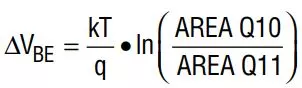
Figure 1: designed band gap circuit provides theoretically zero temperature coefficient
The mathematics behind the basic bandgap reference voltage source is interesting because it combines a known temperature coefficient with a unique resistivity to produce a reference voltage with a theoretical temperature drift of zero. Figure 1 shows the two transistors, adjusted so that the emitter area of Q10 is 10 times that of Q11, while the collector current of Q12 and Q13 remains the same. This creates a known voltage between the two transistor bases:
Where, k is boltzmann constant in J/ k (1.38×10⁻²³), T is kelvin temperature (273+T(°C)). Q is the electron charge in coulombs (1.6x10⁻¹⁹). At 25°C, the value of kT/q is 25.7mV, and the positive temperature coefficient is 86 ° V/°C. ? VBE is this voltage multiplied by ln(10) or 2.3. At 25°C the voltage is approximately 60mV with a temperature coefficient of 0.2mV/°C.
Applying this voltage to the 50k resistance connected between the base produces a current proportional to the temperature. The current offset diode Q14 has a voltage of 575mV and a temperature coefficient of -2.2mV/°C at 25°C. The resistance is used to produce a voltage drop with a positive temperature coefficient applied to the Q14 diode voltage, resulting in a reference voltage potential of approximately 1.235v, with a theoretical temperature coefficient of 0mV/°C. These pressure drops are shown in figure 1. The balance of the circuit provides the offset current and the output drive.
Fractional bandgap reference voltage source
The reference voltage source is based on the temperature characteristics of the bipolar transistor, but the output voltage can be as low as a few mV. It is suitable for ultra low voltage circuits, especially for comparator applications where the threshold must be less than the conventional bandgap voltage (approx. 1.2v).
Figure 2 shows the core circuit of the LM10, which is similar to a normal bandgap reference source, where components proportional and inversely proportional to temperature are combined to obtain a constant 200mV reference voltage. Fractional bandgap reference voltage sources are commonly used. VBE produces a current proportional to temperature, and using VBE produces a current inversely proportional to temperature. The two are combined in an appropriate proportion in a resistance element to produce a voltage that does not vary with temperature. The resistance size can be changed to change the reference voltage without affecting the temperature characteristic. This differs from traditional bandgap circuits in that fractional bandgap circuits combine currents, whereas traditional circuits tend to combine voltages, usually the emitter, the base voltage, and the I? R.
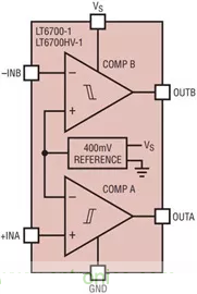 Figure 2:0mV reference voltage source circuit
Fractional bandgap reference voltage sources such as the LM10 circuit are also subtractive in some cases. Some devices have a micropower, low voltage 400mV reference and a series reference of the amplifier. Therefore, the reference voltage can be changed by changing the gain of the amplifier and providing a buffered output. Using this simple circuit can produce any output voltage below the power supply voltage of 0.4v to a few millivolts.
Figure 3: support for comparison with a threshold as low as 400mV
Some devices combine a 400mV reference voltage source with a comparator, which is a more integrated solution and can be used as a voltage monitor or window comparator. The 400mV reference voltage source can monitor small input signals, thus reducing the complexity of the monitoring circuit (figure 3). It can also monitor circuit components operating at very low power voltages. If the threshold is large, a simple resistance divider can be added (figure 4). These products are packaged in small sizes (SOT23), consume very little power (less than 10xa), and support A wide power range (1.4v to 18V).
 Figure 4: a higher threshold is set by input voltage partial voltage
Select the reference voltage source
With all these options in mind, how do you choose the right voltage reference source for your application? Here are some tips to narrow down your options:
● very high power supply voltage? Select the shunt reference voltage source.
● does the supply voltage or load current vary widely? Select a series reference voltage source.
● need a high efficiency ratio? Select a series reference voltage source.
● determine the actual temperature range. Temperatures range from 0°C to 70°C, -40°C to 85°C, and -40°C to 125°C.
● accuracy requirements should be realistic. It is important to understand the precision required for the application. This helps determine key specifications. For this requirement, multiply the temperature drift by the specified temperature range, plus
The overall accuracy is obtained by subtracting any items that will be calibrated at the factory or recalibrated at regular intervals from the initial accuracy error, thermal hysteresis, and long-term drift during the expected product life. For the most demanding applications, noise, voltage adjustment, and load adjustment errors can also be added. Such as:
A reference voltage source has an initial accuracy error of 0.1% (1000ppm), a temperature drift of 25ppm/°C from -40°C to 85°C, a thermal delay of 200ppm, peak-to-peak noise of 2ppm, and a time drift of 50ppm/√kHr.
Then the total uncertainty will exceed 4300ppm when the circuit is built.
In the first 1000 hours after the circuit is energized, this uncertainty increases by 50ppm. The initial precision can be calibrated to reduce the error to 3300ppm+50ppm, right? Square root of t over 1000 hours.
● what is the actual power range? What is the maximum expected supply voltage? Are there any fault conditions that the reference voltage source IC must withstand, such as battery power cut or hot-plug induction power spikes? This can significantly reduce the number of reference sources available.
● what is the potential power consumption of the reference voltage source? Reference voltage sources tend to fall into several categories:
Greater than 1 ma, ~500 moles of A, <300 moles of A, <50 moles of A, <10 moles of A, <1 moles of A.
● how big is the load current? Does the load consume large amounts of current or generate the current that the reference source must absorb? Many reference voltage sources can only provide a small amount of current to the load, and few can absorb a large amount of current. The load adjustment rate specification can effectively illustrate this problem.
● how much installation space is there? The reference voltage source comes in a variety of packages, including metal cap cases, plastic seals (DIP, SOIC, SOT), and very small packages, such as products with 2mmx2mm DFN. It is generally accepted that the error due to mechanical stress of a reference voltage source in a larger package is less than that of a reference voltage source in a smaller package. While there are some reference voltage sources that perform better with larger packages, there is evidence that performance differences are not directly related to package size. More likely, because products in smaller packages use smaller chips, some sort of performance trade-off must be made to fit the circuitry on the chip. Often, the installation method of the package has a greater impact on performance than the actual package, and paying close attention to the installation method and location maximizes performance. In addition, when a PCB is bent, a device with a smaller footprint may have less stress than one with a larger footprint.